A bit of theory with my perspective view how the diffamp works
I decided to separate the article on two parts: MOS and bipolar based amps, it should be more logical if me or somebody else is going through it.
But before the separation, I will shortly list the advantages which are common for both types:
- Doubled swing (in comparison to single mode)
- Common mode rejection
- Power rail noise immunity (power rail noise is subtracted from both arms)
- Neighbor lines noise immunity (again the noise is impacting both arms in a same way)
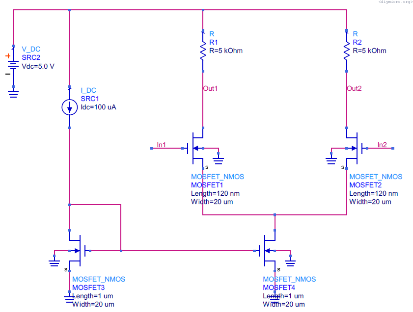
MOS
Lets begin from the allowed DC input level.
Usually I take two ends and analyze them separately. Therefore, starting from the ground end – look at the M4 transistor, to make sure that this guy in saturation we should make his drain voltage larger or equal Vgs4-Vth3, plus we have the diff pair transistor by itself sitting on top of it:
Vcm>=Vgs1+Vgs4-Vth4.
This one was easy, now to the other one, looking to M1 saturation criteria – Vds >=Vgs1-Vth1, rewrite this as:
Vout1 – Vp >= Vcm – Vp – Vth1, from where Vcm <= Vout1 + Vth1 = Vdd – I*R/2 + Vth1.
Therefore, the combined condition is:
Vgs1+Vgs4-Vth4 <= Vcm <= Vdd – I*R/2 + Vth1
Now we can derive the input-output characteristic:
Vout1 – Vout2 = Id1*Rd – Id2*Rd = Rd(Id1 – Id2)
But Vp = Vin1 – Vgs1 = Vin2 – Vgs2, => Vin1 – Vin2 = Vgs1 – Vgs2, so (again, we are in saturation and speaking about long channel only):

If we will try to use Id1 – Id2 in the equation we can derive the Vout:

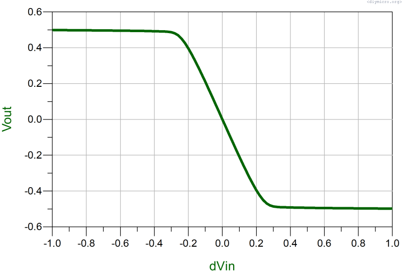
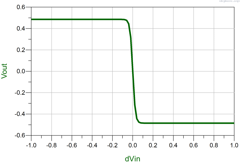
And now let me show Vout for the circuit pictured in the post title:

From this picture we can conclude that the saturation mode is held within -100..+100mV. Out of those margins we have no more current to withdraw and the amplifier from now on is the non-linear mode, the input voltage in the transition region is:

This formula shows quite important thing – if we would like to extend the linear region, we should either increase the current either decrease K (decrease W or increase L).

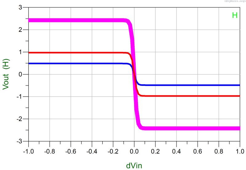
In the picture above I had changed the current from smaller to a larger value (red, blue, pink), the impact is clearly visible.
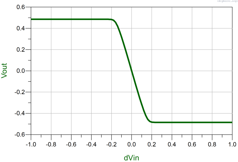
The other solution to extend the linear range – to add source resistors. This will add a negative current feedback and decrease the gain, or equally, will increase the range. The calculation are bit more complex so I just show the example of the amp with 100uA current and 2.5 KOHm resistors added:
The margins are still exactly same, but the slope (=the gain) has changed.
Now let me calculate the gain of the differential amplifier.
Firstly we should agree on one simple rule:
In the symmetric circuit if inputs has been changed on the same values but different polarities , then the common mode voltage (the sources) is not changed and we can assume that it is a ground for small signal calculus
So, if we apply this rule to the differential amplifier than we can divide it on two exactly same common source amplifiers, let me grab picture from Razavi’s book:
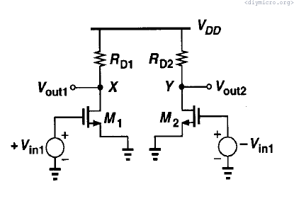
Vout1 = -gm*Rd*Vin1, Vout2 = -gm*Rd*Vin2
Vout1-Vout2 = -gm*Rd*(Vin1-Vin2) -> gain (diff) = -gm*Rd
Simply talking – it matches the gain of the single ended common source version.
So for the source degenerated version we will have also:

Bipolar differential amplifier
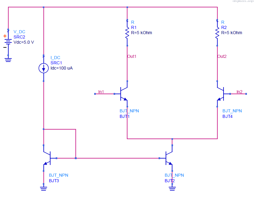
The bare structure is exactly same as for MOS transistors, let me try to break it down in a similar way.
Allowed range for input dc level:
Again, the current source on the bottom side (BJT2), the Vce shouldn’t be larger than Vcesat and the minimum allowed input voltage is Vcesat + Vbe1
On the other side we have:
Vce1 = Vout1-Vin1+Vbe1 > Vcesat
So, Vin < Vout1,2 + Vbe1,4 – Vcesat = Vdd – Ic1,2Rc+Vbe1,4-Vcesat
Откуда Uin1,2 < Uout1,2 + Ube1,4 – Ucesat = Vdd – Ic1,2Rc +Ube1,4 – Ucesat
Now let me derive the output differential voltage
Uout = Uout1 – Uout2 = Rc(Ic2-Ic1)
Uin = Uin1 – Uin2 = Ube1 – Ube2.
Useful hint: Ic2/Ic1 = e^(Uin/Ut)
Gathering everything to one place:

Which on the graph looks like this:
The graph clearly shows that the slope is a way larger in comparison to the MOS version, this is kind of advantage of the bipolar – much easier to get larger gains. The transition point is approximated by:

Which gives us an idea that since it is underneath of the logarithm we would not have the great impact of the current or sizes on the range value.
The experiment above just proven the point, not much of the changing happened.
Thus, the easiest way to get the range increased is to use the emitter resistors and decrease the gain, for instance 100uA and 2.5KOhm resistor:
The gain of bipolar diffamp represented by same equations as for MOS, but take into account that gm of bipolar is I/Vt (dI/dVbe) which has “weaker” dependence on the size of the device.