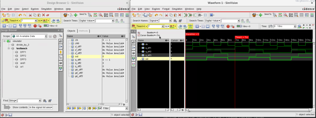
Since I already described the process in my previous post, this one is going to be much shorter.
So, let’s use the same example of the divide by 3 circuit:
In the xcelium case, it is actually easier to runthe testbench somewhat if you are comfortable with the command line interface (CLI):
xrun testbench_sandbox.sv design_sandbox.sv -access +rwc -gui The verilog code is exactly the same as it was in the aforementioned post, but I’m repeating that again.
The module code:
//sandbox design diymicro

module dff (clk, d, q, qb);
  input      clk;
  input      d;
  output     q;
  output     qb;

  reg        q;

  assign qb = ~q;

  initial begin
    q = 1'b0;
  end


  always @(posedge clk)
  begin
      // Assign D to Q on positive clock edge
      q <= d;
  end
endmodule


module and_gate (input wire a,b,
                 output wire z);

  assign z = a & b;

endmodule


module or_gate (input wire a,b,
                 output wire z);

  assign z = a | b;

endmodule
The testbench code:
// Code your testbench here
// or browse Examples

`timescale 1ns / 1ns

module testbench();

  reg clk;
  wire out;
  wire qb_dff1;
  wire d_dff1;
  wire q_dff1;
  wire clkb;
  wire qb_dff2;
  wire d_dff2;
  wire q_dff2;
  wire qb_dff3;
  wire d_dff3;
  wire q_dff3;


  assign clkb = ~clk;

  dff DFF1(.clk(clk), .d(d_dff1), .q(q_dff1), .qb(qb_dff1));
  dff DFF2(.clk(clk), .d(d_dff2), .q(q_dff2), .qb(qb_dff2));
  dff DFF3(.clk(clkb), .d(d_dff3), .q(q_dff3), .qb(qb_dff3));

  and_gate and1(.a(qb_dff1),.b(qb_dff2),.z(d_dff1));

  assign d_dff2 = q_dff1;
  assign d_dff3 = q_dff2;

  or_gate or1(.a(q_dff3),.b(q_dff2),.z(out));

  //assign d_dff1 = qb_dff1;


  initial begin
    $dumpfile("dump.vcd");
    $dumpvars(1);


    clk = 1'b0;

    #18 $finish;

  end

always #1 clk = ~clk;

endmodule : testbench
SimVision will start after that xrun command and you will need to add waveforms of interest to the wave window and click the run button again…